⚠ All product names, trademarks, brands, and logos on this site are the property of their respective owners. Their use is for identification purposes only and does not imply any affiliation or authorization from the rights holders. We are not authorized dealers or distributors of the brand. The warranty is provided by us, not the original manufacturer.
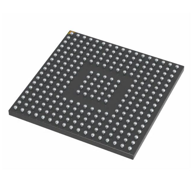
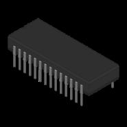
SSTV16859EC
SSTV16859EC - Brand New PHILIPS Special Logic ICs


 Credit Card
 - One-month free return and one year warranty.
- Full or Partial Refund, if the item is not as described
- Full Refund if you don't receive your order
DESCRIPTION
The SSTV16859 is a 13-bit to 26-bit SSTL_2 registered driver with differential
clock inputs, designed to operate between 2.3 V and 2.7 V. All inputs are
compatible with the JEDEC standard for SSTL_2 with VREF normally at 0.5*VDD,
except the LVCMOS reset (RESET) input. All outputs are SSTL_2, Class II
compatible which can be used for standard stub-series applications or
capacitive loads. Master reset (RESET) asynchronously resets all registers to
zero.
The SSTV16859 is intended to be incorporated into standard DIMM (Dual In-Line
Memory Module) designs defined by JEDEC, such as DDR (Double Data Rate) SDRAM
and SDRAM II Memory Modules. Different from traditional SDRAM, DDR SDRAM
transfers data on both clock edges (rising and falling), thus doubling the
peak bus bandwidth. A DDR DRAM rated at 133 MHz will have a burst rate of 266
MHz.
The device data inputs consist of different receivers. One differential input
is tied to the input pin while the other is tied to a reference input pad,
which is shared by all inputs.
The clock input is fully differential (CK and CK) to be compatible with DRAM
devices that are installed on the DIMM. Data are registered at the crossing of
CK going high, and CK going low. However, since the control inputs to the
SDRAM change at only half the data rate, the device must only change state on
the positive transition of the CK signal. In order to be able to provide
defined outputs from the device even before a stable clock has been supplied,
the device has an asynchronous input pin (RESET), which when held to the LOW
state, resets all registers and all outputs to the LOW state.
The device supports low-power standby operation. When RESET is low, the
differential input receivers are disabled, and undriven (floating) data,
clock, and reference voltage (VREF) inputs are allowed. In addition, when
RESET is low, all registers are reset, and all outputs are forced low. The
LVCMOS RESET input must always be held at a valid logic high or low level.
To ensure defined outputs from the register before a stable clock has been
supplied, RESET must be held in the low state during power-up.
In the DDR DIMM application, RESET is specified to be completely asynchronous
with respect to CK and CK. Therefore, no timing relationship can be guaranteed
between the two. When entering RESET, the register will be cleared and the
outputs will be driven low. As long as the data inputs are low, and the clock
is stable during the time from the low-to-high transition of RESET until the
input receivers are fully enabled, the outputs will remain low.
Available in 64-pin plastic thin shrink small outline package.
FEATURES
• Stub-series terminated logic for 2.5 V VDD (SSTL_2)
• Optimized for stacked DDR (Double Data Rate) SDRAM
applications
• Supports SSTL_2 signal inputs as per JESD 8–9
• Flow-through architecture optimizes PCB layout
• ESD classification testing is done to JEDEC Standard JESD22.
Protection exceeds 2000 V to HBM per method A114.
• Latch-up testing is done to JEDEC Standard JESD78, which
exceeds 100 mA.
• Supports efficient low power standby operation
• Full DDR 200/266 solution for stacked DIMMs at 2.5 V when used
with PCKV857
• See SSTV16857 for JEDEC compliant register support in
unstacked DIMM applications
• See SSTV16856 for driver/buffer version with mode select.
Shipping
| First item | Additional item | Service | Description |
|---|---|---|---|
| $0.00 | Free | Free Shipping | Estimated 15-30 business days via Registered Air Mail or others |
| $27.50 | Free | Expedited Shipping | Estimated delivery time is 3-5 business days, with some areas possibly taking 6-9 business days depending on the shipping address. The main courier companies include but are not limited to UPS, DHL, and FedEx. |
| $0.00 | Free | Buyer cooperating carrier | Using buyer's cooperating carrier. Buyer should create a shipping label and share it to us. And then we will call carrier for pickup |
| $38.00 | Free | Expedited Shipping | Estimated delivery time is 3-5 business days, with some areas possibly taking 6-9 business days depending on the shipping address. The main courier companies include but are not limited to UPS, DHL, and FedEx. |
Delivery
- The transportation time may be delayed due to customs clearance, local holidays or abnormal events.
- The estimated time is based on the fastest speed provided by commercial couriers (DHL, FedEx, UPS etc).
- The estimated time does not include the lead time of the item. The lead time of most items is 2–5 business days. If more than 5 working days are needed, we will manually confirm with you.
| Flag | Country | Express Delivery | Standard Delivery |
|---|---|---|---|
 | United States | 3 - 5 days | 10-15 days |
 | Canada | 3 - 5 days | 10-20 days |
 | Mexico | 3 - 5 days | 10-17 days |
 | Germany | 3 - 5 days | 10-12 days |
 | Italy | 3 - 5 days | 10-15 days |
 | United Kingdom | 3 - 5 days | 10-12 days |
Estimated Delivery
This item requires 2-5 business days for processing before shipping after payment is confirmed. And depending on the destination and shipping method.
Return Policy
| Return window | Refund type | Return shipping |
|---|---|---|
| 60 days after receiving item | Money Back or Replacement | Buyer pays for return shipping |
电子元器件与工控产品的真实买家评价
 In Stock
 100EP17
100EP17 - Brand New ON Semiconductor Special Logic ICs
 In Stock
 32864AH
32864AH - Brand New Littelfuse Special Logic ICs
 In Stock
 4007UBE
4007UBE - Brand New Texas Instruments Special Logic ICs
 In Stock
 7497N
7497N - Brand New NS/TI Special Logic ICs
 In Stock
 74ABT18245ADGGRE4
74ABT18245ADGGRE4 - Brand New Texas Instruments Special Logic ICs
 In Stock
 74ABT899A
74ABT899A - Brand New PHI Special Logic ICs
 In Stock
 74ABT899C
74ABT899C - Brand New onsemi Special Logic ICs
 In Stock
 74ABT899CQCX
74ABT899CQCX - Brand New onsemi Special Logic ICs
 In Stock
 74ABT899CSC
74ABT899CSC - Brand New onsemi Special Logic ICs
 In Stock
 74ABT899CSCX
74ABT899CSCX - Brand New onsemi Special Logic ICs